C1902 V2 Introduction
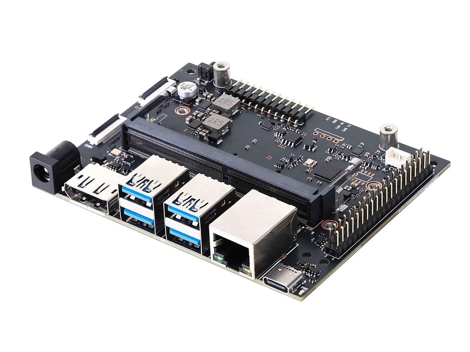
Overview
The C1902 V2 is an industrial-grade carrier board developed for Jetson Orin Nano and NX modules. It is a redesign of the reference carrier board with industrial-grade component optimization, offering better stability and reliability while remaining compatible with the official developer kit.
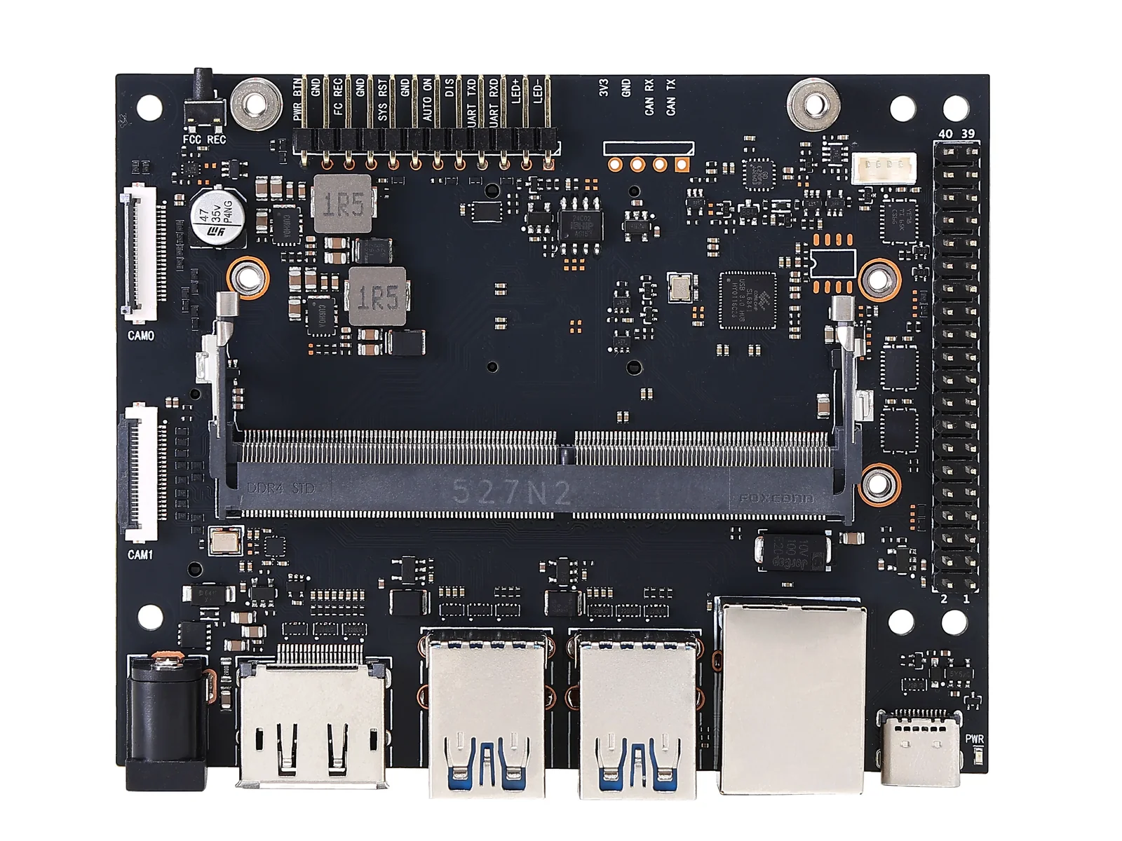
Front
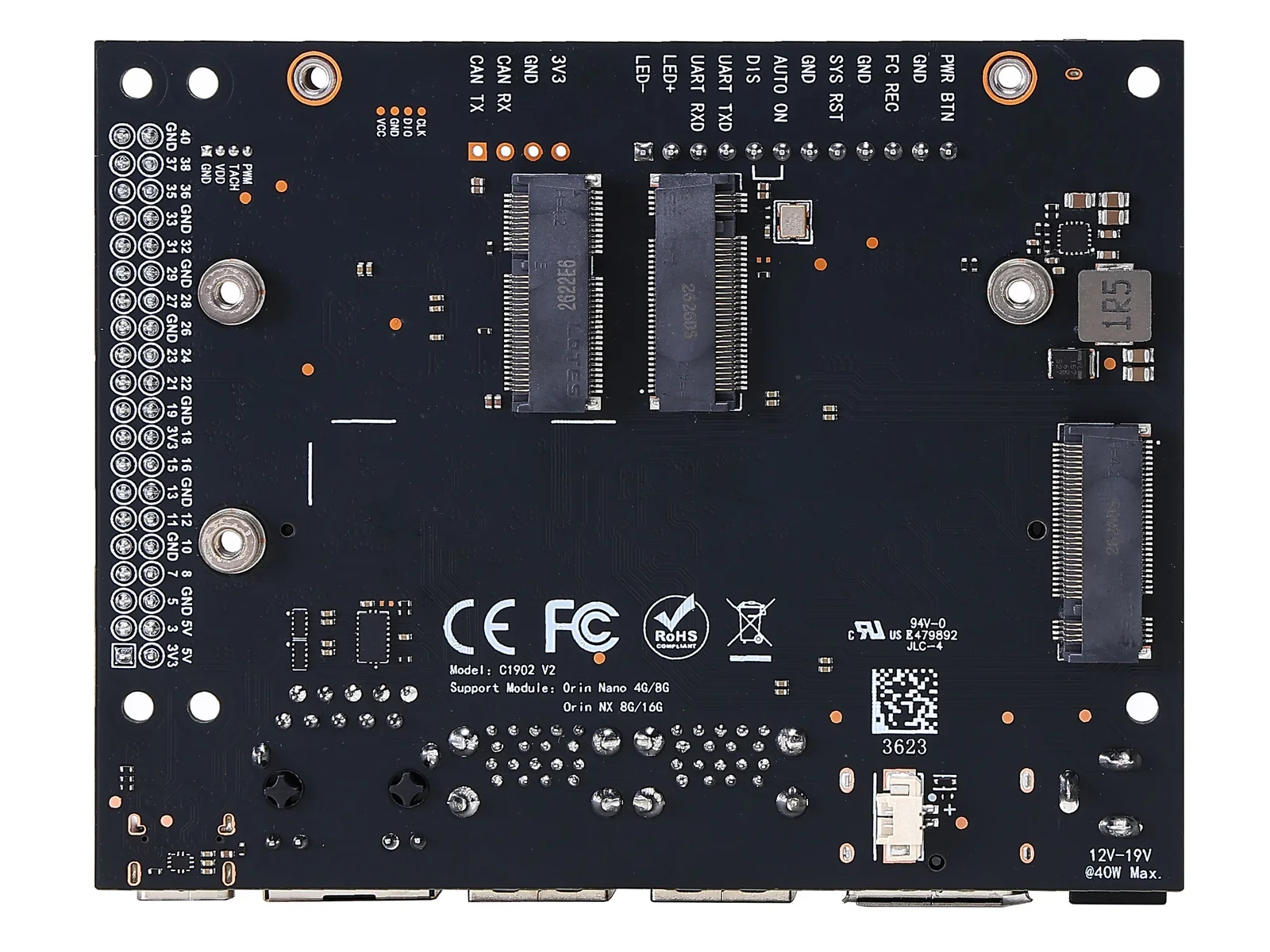
Back
Features
- Based on the reference design: every interface matches the official board, and the Developer Kit firmware can be flashed directly
- Full SUPER mode support for Orin Nano 4GB/8GB and Orin NX 8GB/16GB
- Redesigned power supply for lower heat and higher efficiency
- High-quality 8-layer PCB with strict impedance control on all traces
- Basic industrial temperature range for better stability and reliability
Specifications
| Item | Specification |
|---|---|
| Input voltage | 12V (9V–19V compatible) |
| Power connector | DC5525 |
| Supported modules | Jetson Orin Nano 4GB/8GB, Jetson Orin NX 8GB/16GB |
| Ethernet | 1 × Gigabit RJ45 |
| Wireless | 1 × M.2 Key E |
| Storage | 2 × M.2 Key M (NVMe SSD) |
| Display | 1 × DisplayPort 1.2 |
| USB | 4 × USB 3.2 Type-A (5Gbps) |
| USB-C | 1 × USB 3.2 Type-C (10Gbps) |
| Camera | 2 × CSI, 22-pin |
| Other interfaces | Same as the reference board, plus a 12-pin button/debug header, fan header and REC button |
| RTC battery | Supported, MX1.25-2P, 3V |
| PoE | Not supported |
| Operating temperature | -20℃–55℃ |
- A 12V supply is recommended; 9V–19V input is supported. Make sure the supply provides enough power.
- Improve cooling when the input is above 15V under heavy load.
- The board has reverse-polarity protection on the power input, but do not reverse the supply.
- Each USB port group supplies up to 2.5A; USB power is cut off on overcurrent.
- The M.2 Key E and M.2 2230 slots on the back are mirrored compared with the reference board.
- Only insert or remove the module when the board is powered off.
- Use single-sided SSDs only; double-sided SSDs may collide with the board or short-circuit.
Revision History
| Version | Date | Notes |
|---|---|---|
| V2.0 | 2026 Q3 | Upgraded to industrial grade; the former PWR button changed to REC |
For V1.x boards, see C1902 Introduction.
Comparison
| Item | Reference board | C1902 V1.1.1 | C1902 V2 |
|---|---|---|---|
| Temperature grade | Consumer | Consumer | Industrial |
| Operating temperature | 0℃–45℃ | 0℃–45℃ | -20℃–55℃ |
| Input voltage | 19V | 12V (9–19V compatible) | 12V (9–19V compatible) |
| Power connector | DC5525 | DC5525 | DC5525 |
| Ethernet | 1 × Gigabit (RJ45) | 1 × Gigabit (RJ45) | 1 × Gigabit (RJ45) |
| Wireless | 1 × M.2 Key E | 1 × M.2 Key E | 1 × M.2 Key E |
| Storage | 2 × M.2 Key M | 2 × M.2 Key M | 2 × M.2 Key M |
| Display | 1 × DP 1.2 | 1 × DP 1.2 | 1 × DP 1.2 |
| USB | 4 × USB 3.2 (10Gbps) | 4 × USB 3.2 (10Gbps) | 4 × USB 3.2 (5Gbps) |
| USB-C | 1 × Type-C (USB 3.0) | 1 × Type-C (USB 3.0) | 1 × Type-C (USB 3.2) |
| Camera | 2 × CSI-22P | 2 × CSI-22P | 2 × CSI-22P |
| RTC battery | Not supported | Supported | Supported |
| PoE | Supported (not populated) | Not supported | Not supported |
| SUPER mode | Orin Nano series only | Full Orin Nano / NX lineup | Full Orin Nano / NX lineup |
| Other interfaces | Reference | Same as reference | Same as reference |
Interface Layout
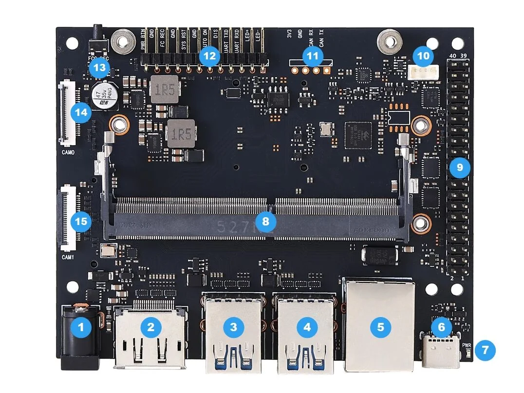
Front
| No. | Name | Notes |
|---|---|---|
| 1 | Power input | DC5525 |
| 2 | DisplayPort | DP 1.2 |
| 3–4 | USB Type-A | 4 × USB 3.2, dual stacked connectors |
| 5 | Ethernet | Gigabit RJ45 |
| 6 | USB Type-C | USB 3.2, used for flashing firmware |
| 7 | Power LED | PWR LED |
| 8 | Jetson Orin module connector | SO-DIMM, 260-pin |
| 9 | 40-pin expansion header | I²C / SPI / UART / GPIO |
| 10 | Fan header | 4-pin, PWM speed control |
| 11 | CAN header | CAN RX / CAN TX, not populated |
| 12 | 12-pin button / debug header | 2.54 mm pitch, includes UART, REC, PWR and other signals |
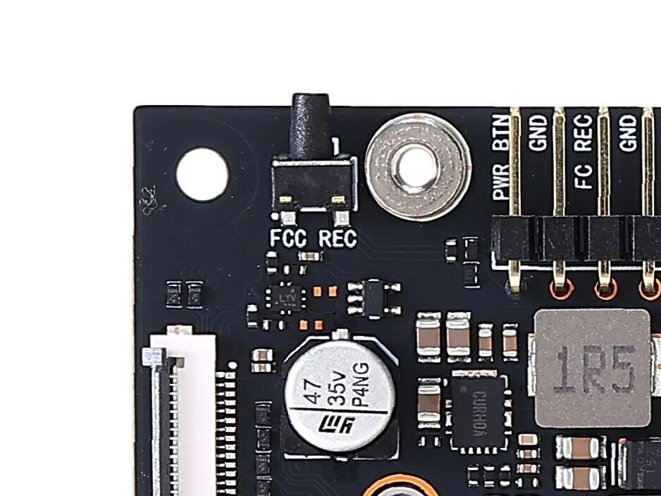
| 13 | REC button | Force Recovery / REC, enters recovery mode |
| 14 | CSI camera connector CAM0 | 22-pin, 0.5 mm |
| 15 | CSI camera connector CAM1 | 22-pin, 0.5 mm |
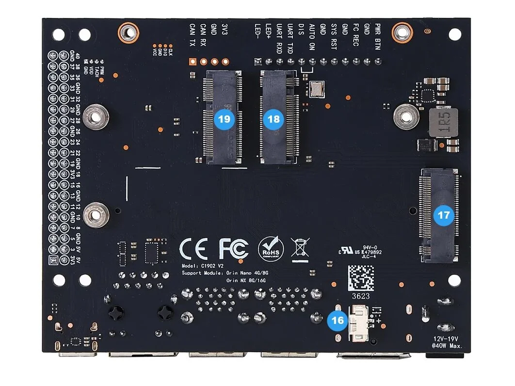
Back
| No. | Name | Notes |
|---|---|---|
| 16 | RTC backup battery connector | MX1.25-2P, 3V |
| 17 | M.2 Key M | 2280, 4-lane |
| 18 | M.2 Key M | 2230, 2-lane |
| 19 | M.2 Key E | 2230 |
Selected Features and Interfaces
Power Input (1)
DC5525 power connector. 12V input is recommended; 9V–19V is supported. Improve cooling above 15V under heavy load.
REC Button (13)
- With the system powered off: hold the button while applying power to enter recovery mode.
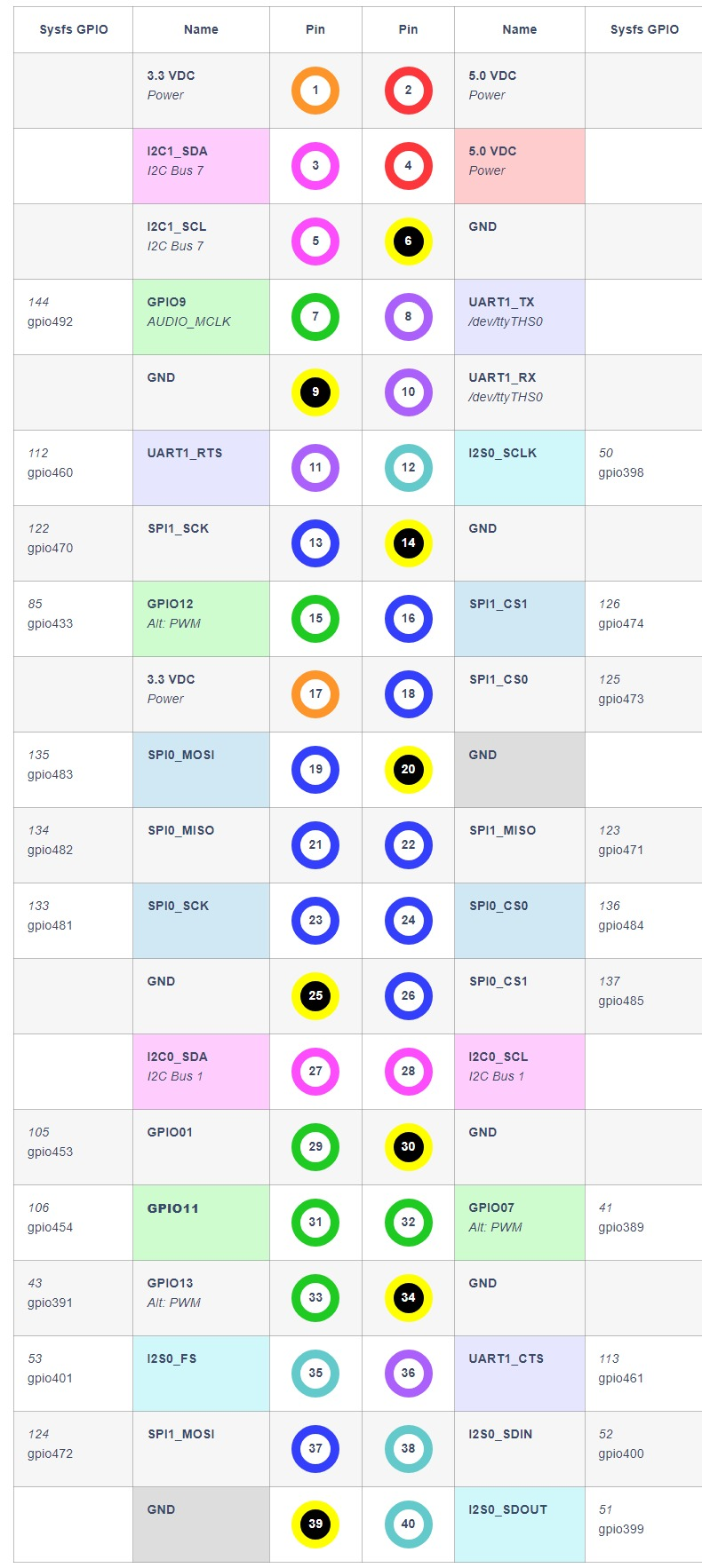
40-pin Expansion Header (9)
The 5V output on the 40-pin GPIO header has back-feed protection and supplies up to 0.8A; it shuts off on overcurrent. Pin functions depend on the module in use.
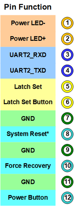
12-pin Button/Debug Header (12)
The header carries power LED, UART, Latch Set, system reset, force recovery and power button signals. The pinout is shown below:
RTC Battery Connector (16)
The connector is an MX1.25-2P and takes a 3V battery. Check the polarity when connecting; never reverse it.
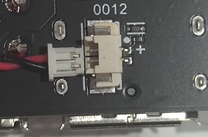
The RTC clock must be configured after the battery is installed. See RTC Interface.
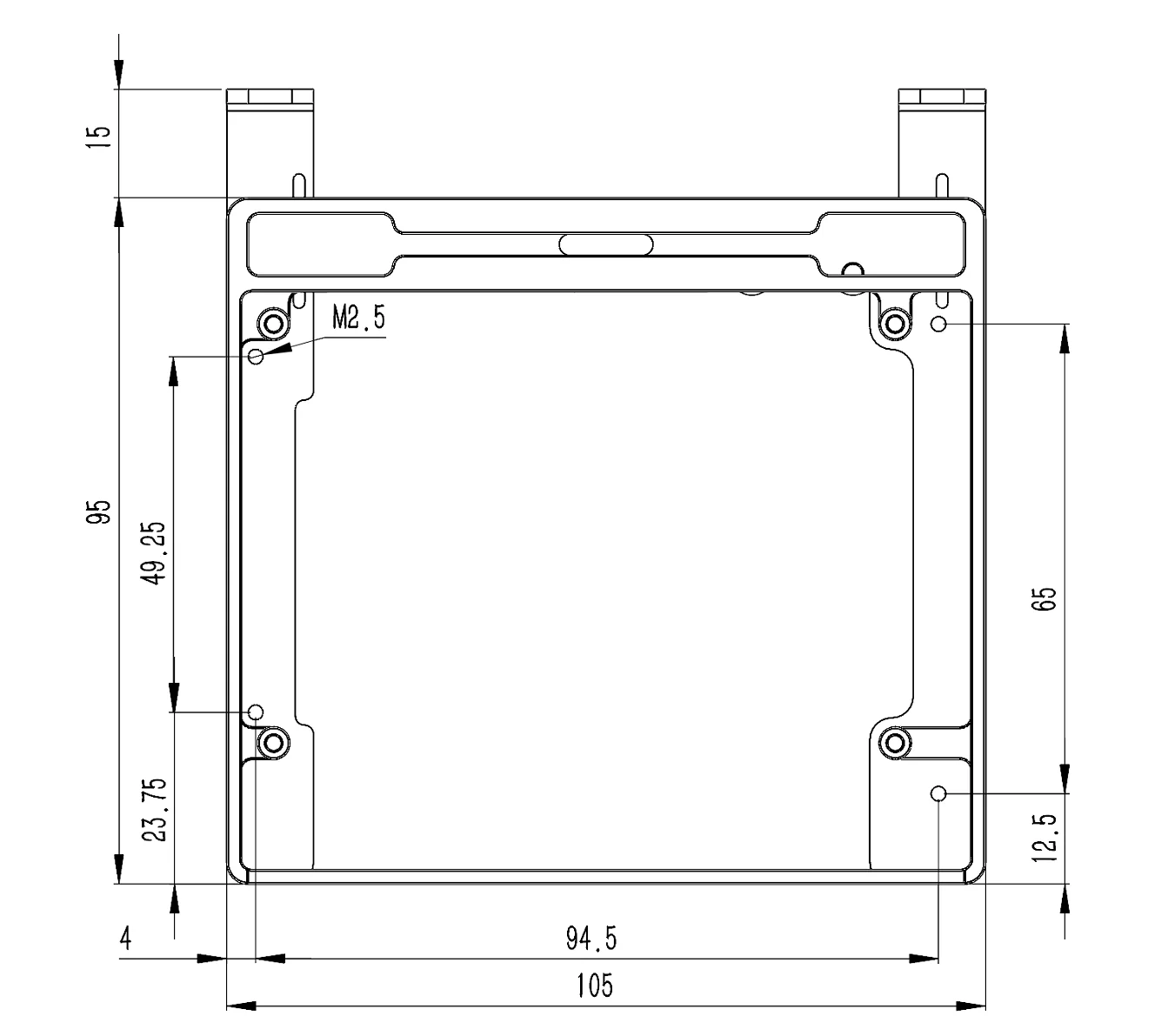
Dimensions (mm)
| Screw location | Recommended | Notes |
|---|---|---|
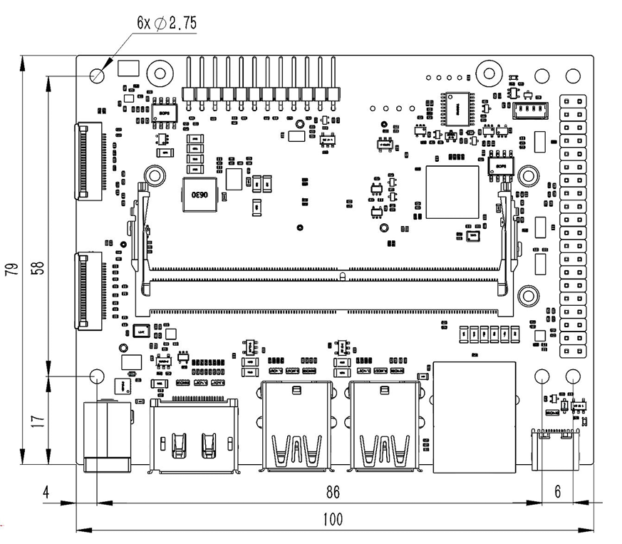
| Board mounting holes | M2.5 screws or standoffs | Diameter ≤ 6mm |
| Module / SSD | M2.5 × 4 low-profile screws | — |
| Wireless card | M2.5 × 4 low-profile screws | — |
Aluminum Base Mounting Holes