
C1903 Introduction
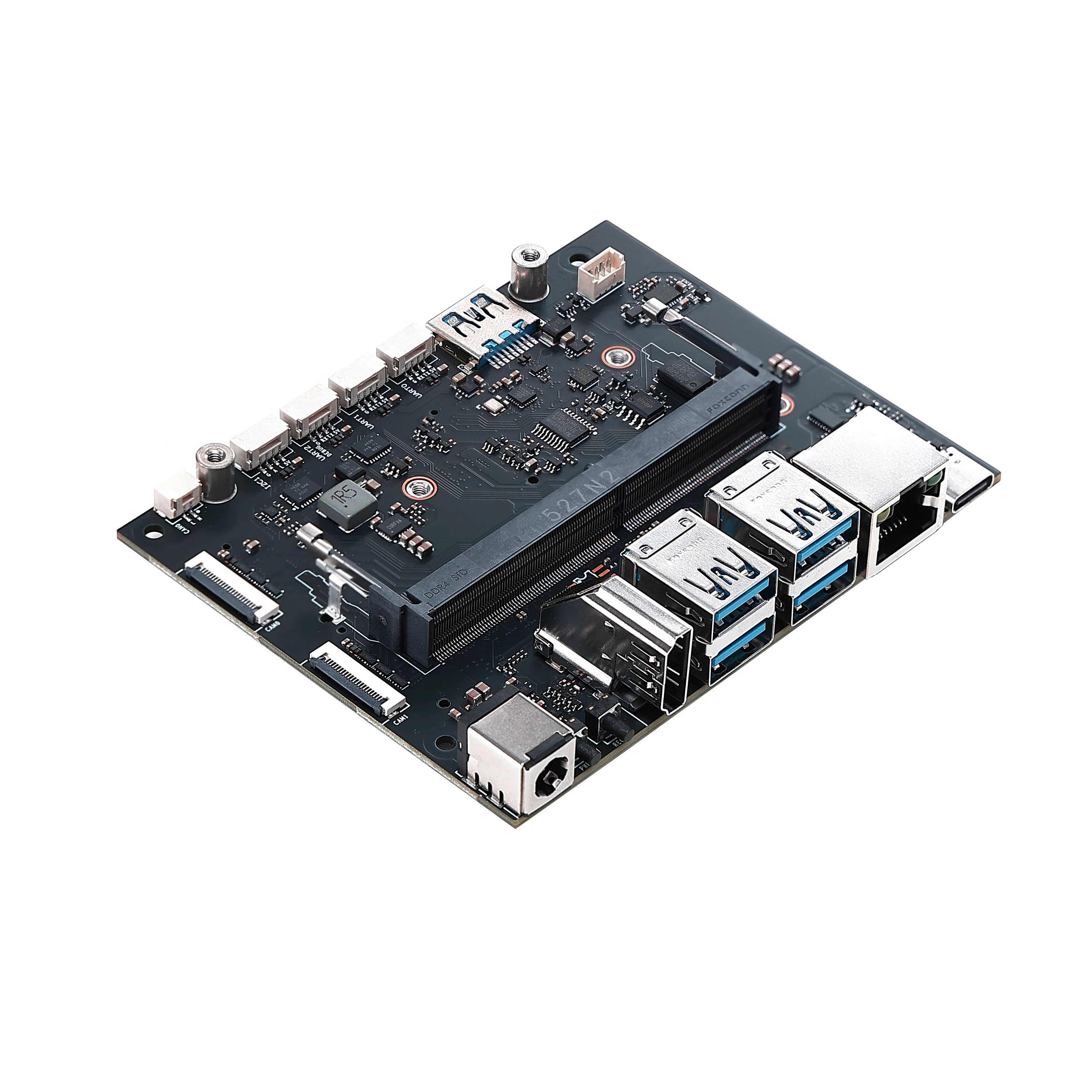
Figure 1. C1903 kit
Safety and Usage Notes
- Use the interfaces and power cable as described in this document to avoid damaging the cable or carrier board.
- Before use, inspect the power cable for aging or damage. Replace it if either condition is found.
- Operate the product only within the specified conditions, including input voltage and temperature. The customer is responsible for damage caused by improper operation.
- Secure the carrier board correctly with screws that meet the stated requirements to prevent damage.
- Disconnect power immediately if sparks, smoke, a burnt smell, or any other abnormal condition is observed after power-on.
Revision History
| Version | Date | Notes |
|---|---|---|
| V1.0 | 2026 Q2 | Initial C1903 release |
Table 1. Revision history
Overview
The C1903 is an industrial-grade carrier board optimized from NVIDIA's reference design. Components are selected to meet at least entry-level industrial-grade requirements, and commonly used interfaces are brought out for easy integration. Its optimized power design supports SUPER mode across the complete Jetson Orin Nano and Orin NX module families.
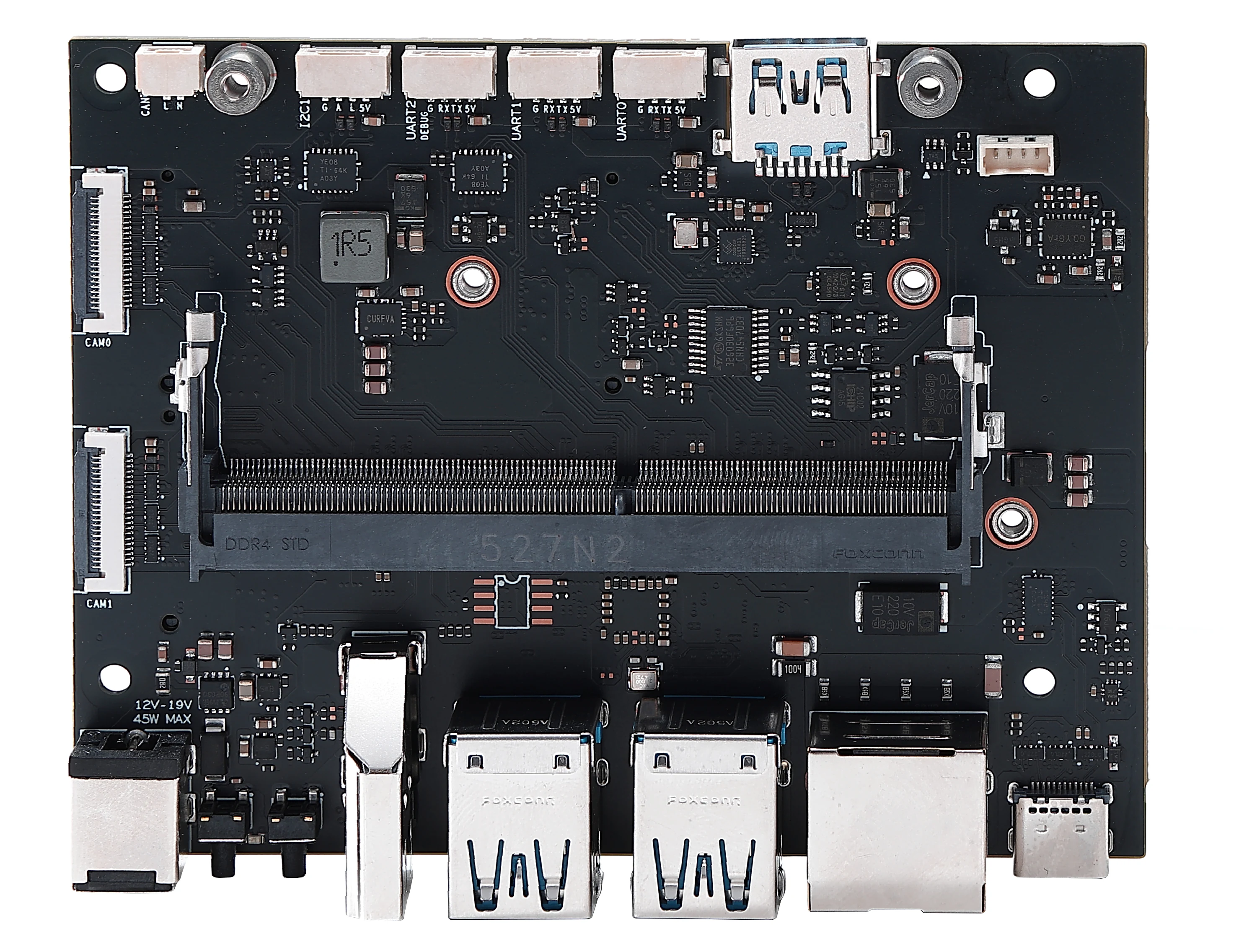
Figure 2. C1903 carrier board, front
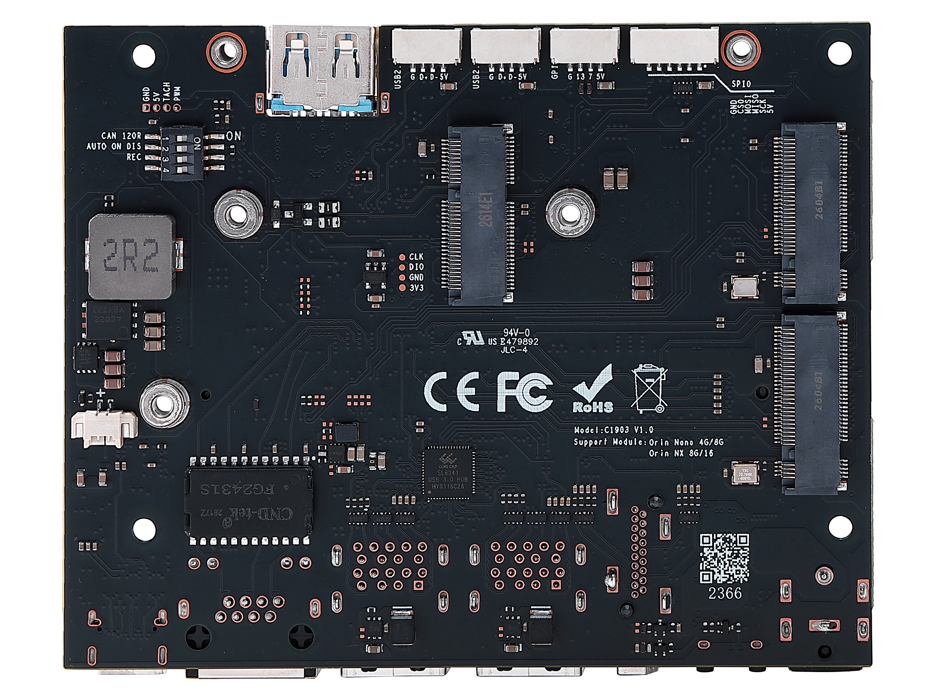
Figure 3. C1903 carrier board, back
Features
- All carrier-board components are selected to at least entry-level industrial-grade specifications for higher reliability and a wider operating-temperature range.
- The complete power path, from the connector to the power-management ICs, is optimized to support SUPER mode across the full Orin Nano/NX family.
- Newly designed 8-layer PCB with strict impedance control on all relevant traces.
- Expanded interface set compared with the reference design, including one additional native USB 3.0 port and two standard USB 2.0 connectors.
Specifications
| Parameter | Value |
|---|---|
| Supply voltage | 12 V nominal (9.5–19 V) |
| Power connector | DC5525 |
| Supported modules | Orin Nano 4GB/8GB, Orin NX 8GB/16GB |
| Ethernet | 1x Gigabit Ethernet |
| Wireless | 1x M.2 Key E (2230) |
| Storage expansion | 1x M.2 Key M (2230), 1x M.2 Key M (2280) |
| Display | 1x HDMI 2.1 |
| USB | 4x USB 3.0 (5 Gbps), 1x USB 3.0 (10 Gbps) |
| USB-C | 1x Type-C (USB 2.0), for firmware flashing |
| Camera | 2x 22-pin CSI |
| Other interfaces | UART, CAN, I2C, SPI |
| RTC battery | 1x RTC backup-battery connector |
| Operating temperature | -20℃ to 50℃ |
Table 2. Product specifications
Notes
- The board accepts 12 V nominal input over a 9.5–19 V range. Improve cooling when the input exceeds 15 V.
- Reverse-polarity protection is provided on the power input.
- Maximum output current per USB group is 2.5 A.
- Never insert or remove the Jetson module while the carrier board is powered.
Interface Layout
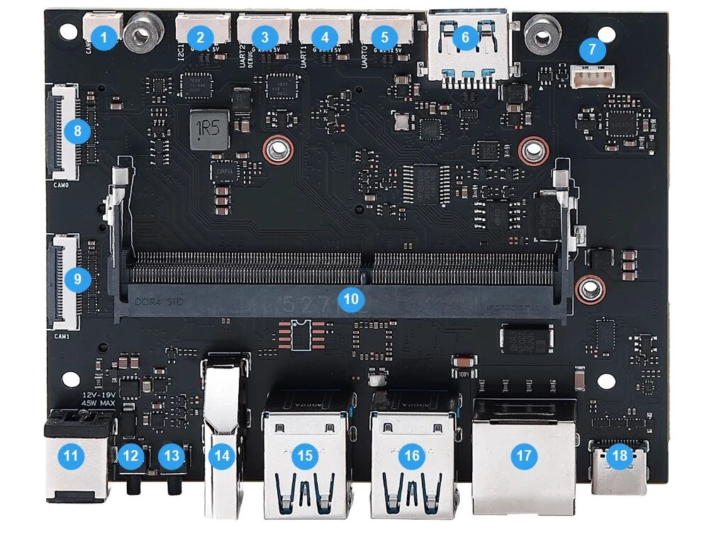
Figure 4. C1903 front interface layout
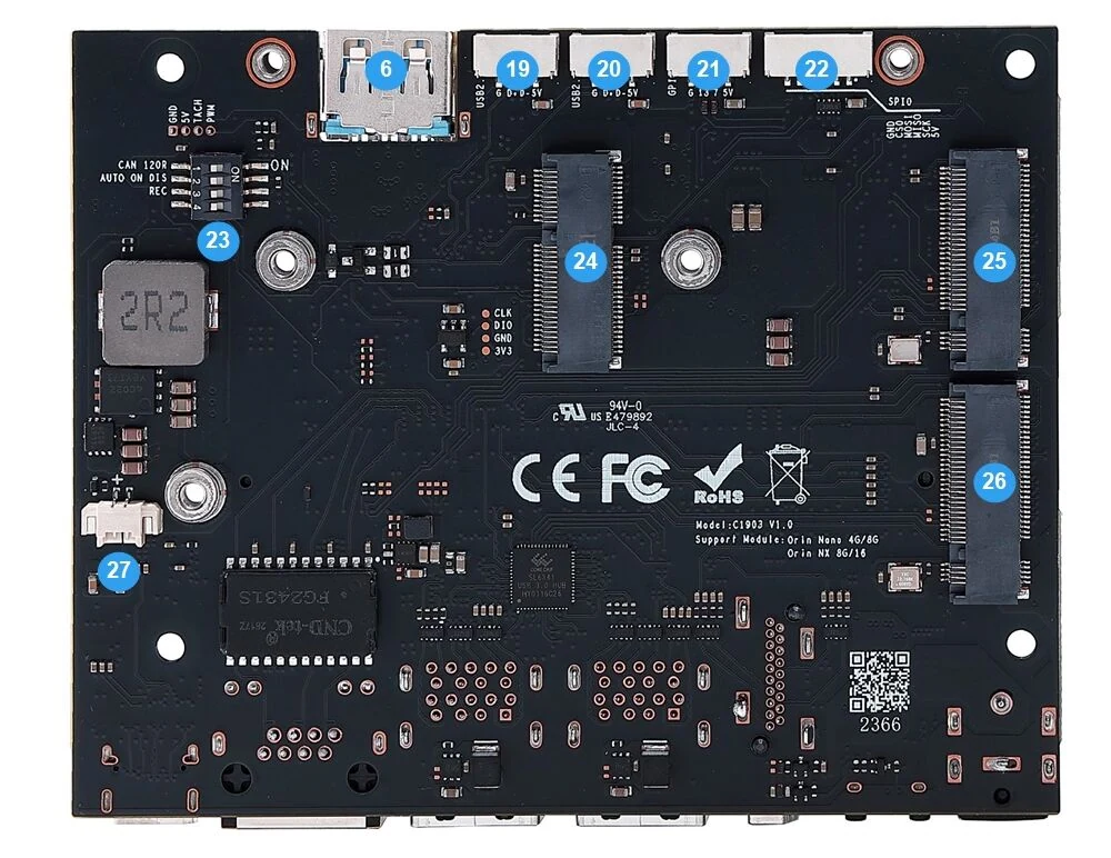
Figure 5. C1903 back interface layout
| No. | Name | No. | Name |
|---|---|---|---|
| 1 | CAN0 (GH1.25 2-pin) | 15 | Stacked USB 3.0 Type-A (5 Gbps) |
| 2 | I2C (GH1.25 4-pin) | 16 | Stacked USB 3.0 Type-A (5 Gbps) |
| 3 | UART2 Debug (GH1.25 4-pin) | 17 | RJ45 Gigabit Ethernet |
| 4 | UART1 (GH1.25 4-pin) | 18 | USB Type-C (USB 3.0, 10 Gbps) |
| 5 | UART0 (GH1.25 4-pin) | 19 | USB 2.0 (GH1.25 4-pin) |
| 6 | USB 3.0 Type-A (10 Gbps, direct from module) | 20 | USB 2.0 (GH1.25 4-pin) |
| 7 | PWM fan connector | 21 | GPIO (GH1.25 4-pin) |
| 8 | CSI0 | 22 | SPI0 (GH1.25 6-pin) |
| 9 | CSI1 | 23 | Function DIP switch |
| 10 | Jetson Orin module socket (SO-DIMM) | 24 | M.2 E-Key (2230) |
| 11 | DC5525 power connector | 25 | M.2 M-Key (2230) |
| 12 | Power button | 26 | M.2 M-Key (2280) |
| 13 | REC button | 27 | RTC battery connector |
| 14 | HDMI |
Table 3. Interface layout
- USB 3.0 Type-A (No. 6): This USB 3.0 port is routed directly from the Jetson module. The device tree must be replaced before the port can be used. See USB Configuration for instructions.
Selected Functions and Interfaces
DC5525 Power Input
The recommended input is 12 V, with a supported range of 9.5–19 V. Improve cooling under high load when the input voltage exceeds 15 V.
| Module | Recommended power |
|---|---|
| Orin Nano 4GB/8GB | 45 W |
| Orin NX 8GB/16GB | 60 W |
Table 4. Recommended power-supply ratings
Power and REC Buttons
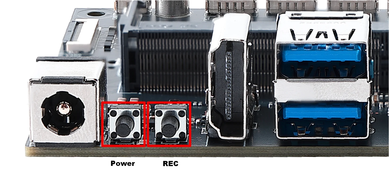
Figure 6. Power and REC buttons
- Enter recovery mode: With power disconnected, hold the REC button and then apply power. Alternatively, set DIP switch 3 to ON to enter recovery mode automatically at every power-on.
- Power button: While the system is on, press once to shut down or hold for 10 seconds to force power-off. While the system is off, press once to power on.
- Set DIP switch 2 to ON to disable automatic power-on.
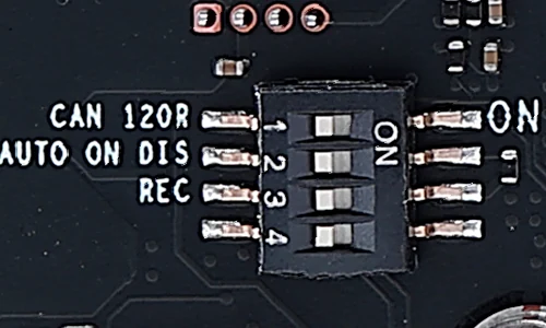
Figure 7. Function DIP switch
GH1.25 Peripheral Connectors
Selected signals are brought out through GH1.25 connectors. The pin definitions are listed below. When viewing each connector from the direction shown, pin numbers run from left to right.
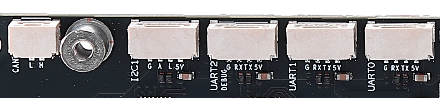
Figure 8. GH1.25 peripheral connectors, front
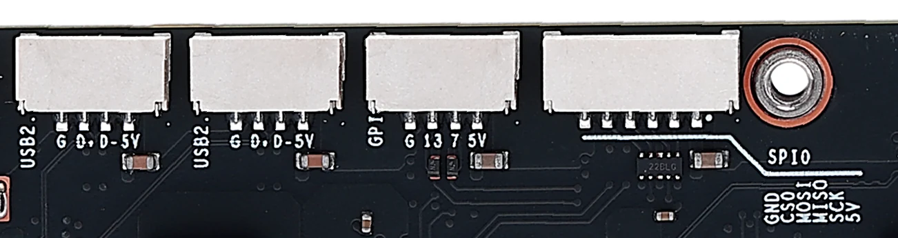
Figure 9. GH1.25 peripheral connectors, back
| Interface | Pin 1 | Pin 2 | Pin 3 | Pin 4 | Pin 5 | Pin 6 |
|---|---|---|---|---|---|---|
| CAN0 | CAN_L | CAN_H | — | — | — | — |
| I2C | GND | SDA | SCL | 5V | — | — |
| UART2 Debug | GND | RX | TX | 5V | — | — |
| UART1 | GND | RX | TX | 5V | — | — |
| UART0 | GND | RX | TX | 5V | — | — |
| USB2.0-1 | GND | D+ | D− | 5V | — | — |
| USB2.0-2 | GND | D+ | D− | 5V | — | — |
| GPIO | GND | GPIO13 | GPIO7 | 5V | — | — |
| SPI0 | GND | CS0 | MOSI | MISO | SCK | 5V |
Table 5. GH1.25 peripheral connector pinout
RJ45 Ethernet
- Gigabit Ethernet (No. 17): RTL8111 controller; no additional driver is required.
Dimensions
Carrier Board Dimensions
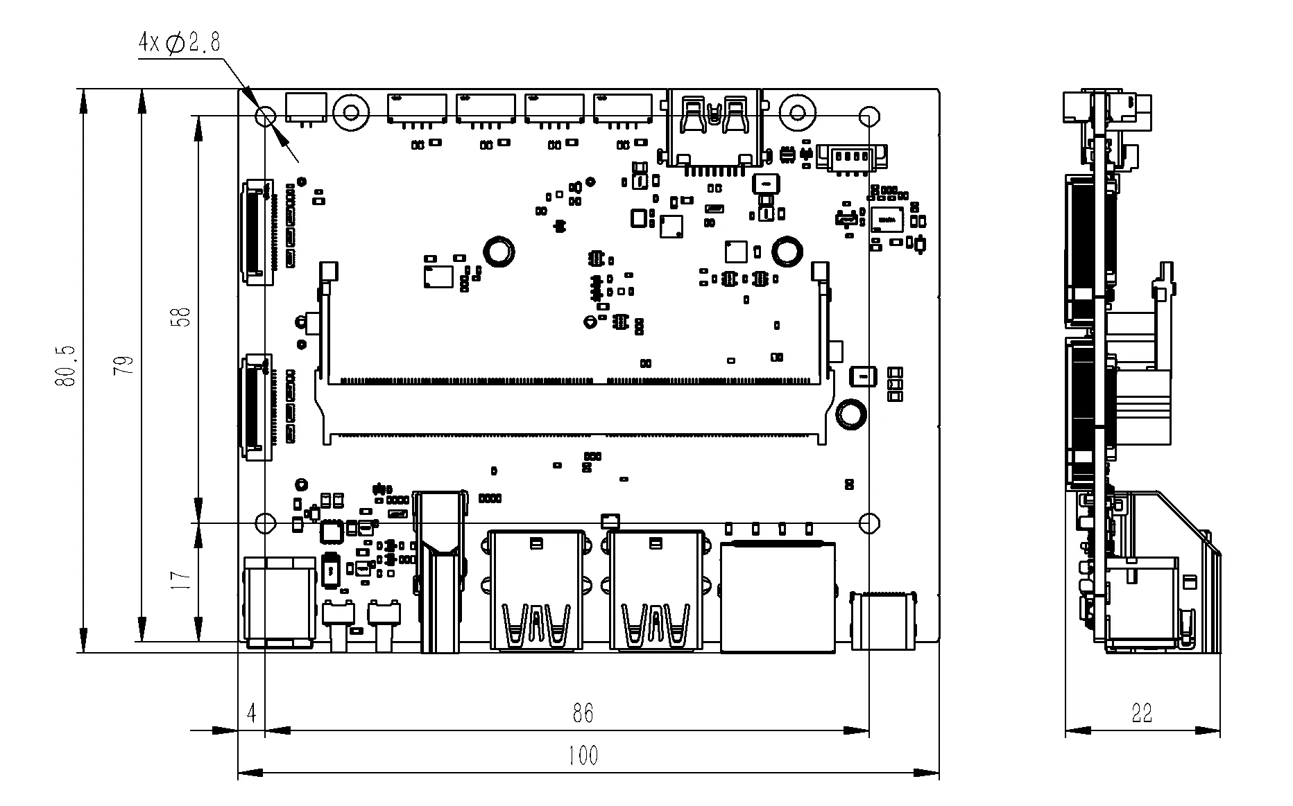
Figure 10. C1903 carrier-board dimensions (top and side views)
| Location | Recommended screw | Notes |
|---|---|---|
| Carrier-board mounting holes | M2 screw or standoff | Maximum head diameter ≤ 4.5 mm |
| Jetson module | M2.5 x 4 low-profile screw | Maximum head diameter ≤ 5 mm |
| M.2 connector | M2.5 x 4 low-profile screw | Maximum head diameter ≤ 5 mm |
Table 6. Carrier-board fastener requirements
Kit Dimensions
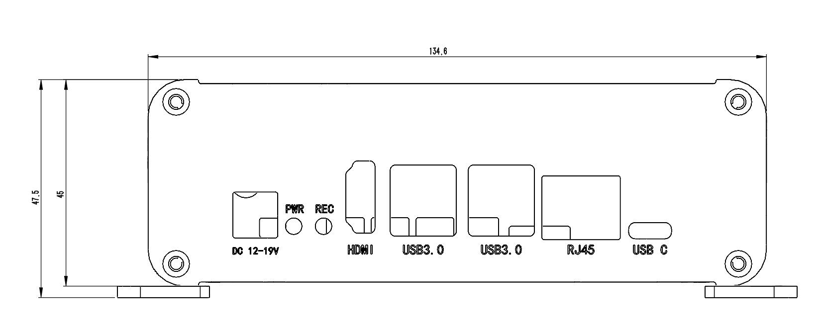
Figure 11. C1903 kit front dimensions
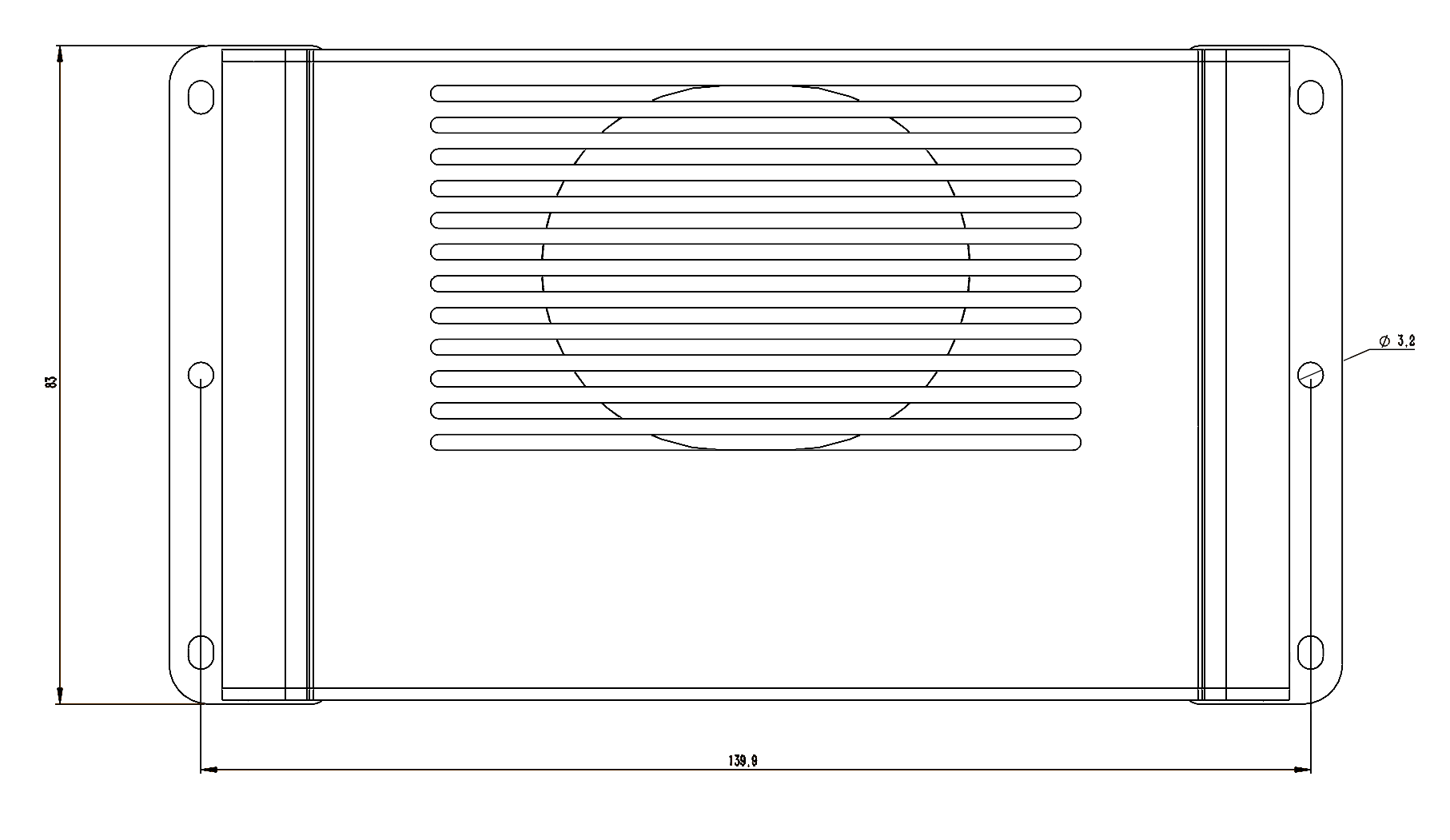
Figure 12. C1903 kit top dimensions
More Views
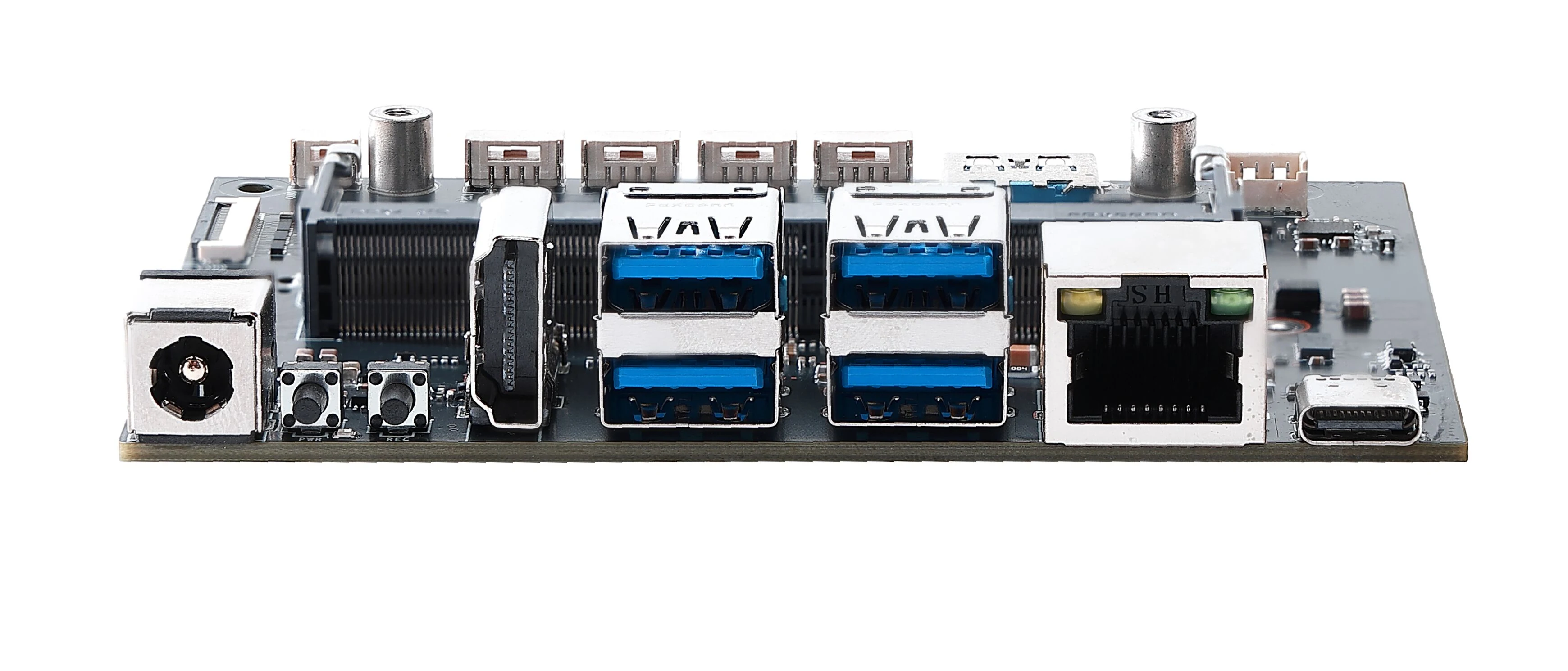
Figure 13. C1903 carrier-board front view
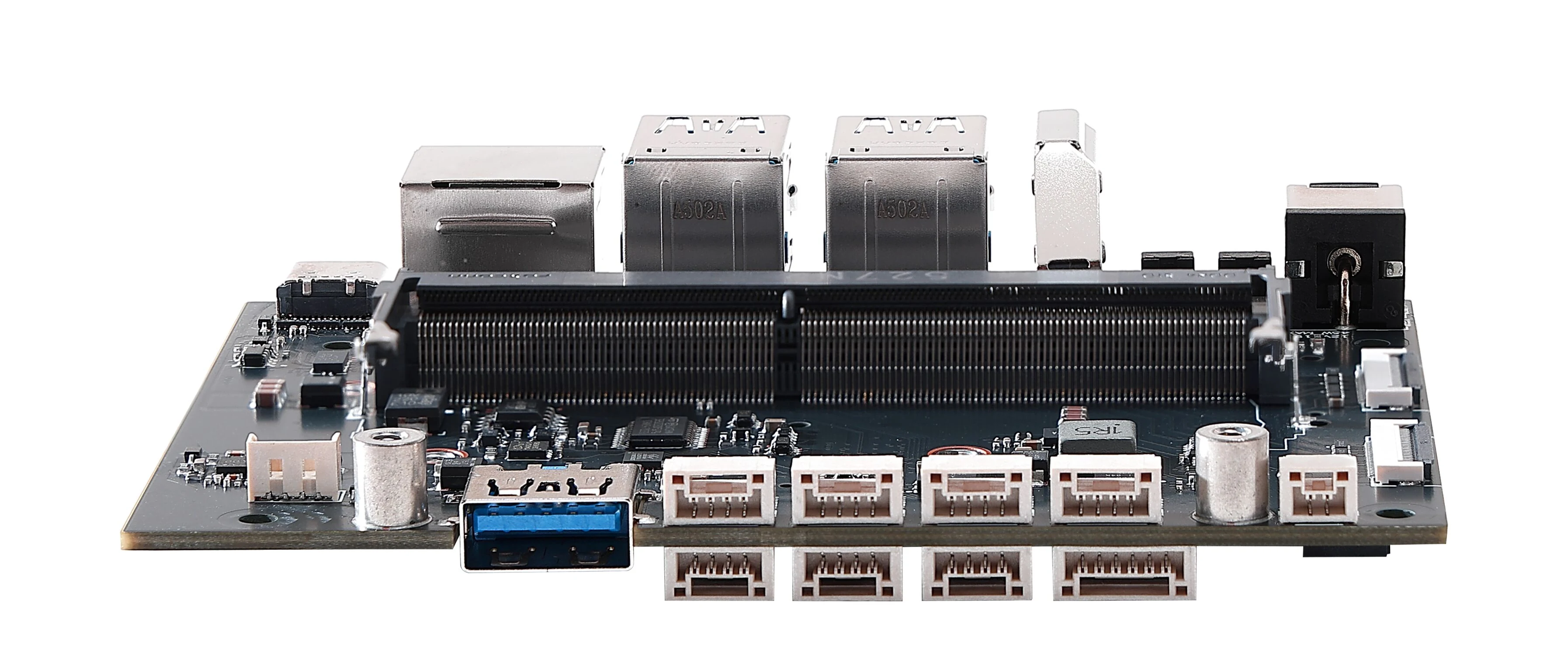
Figure 14. C1903 carrier-board back view
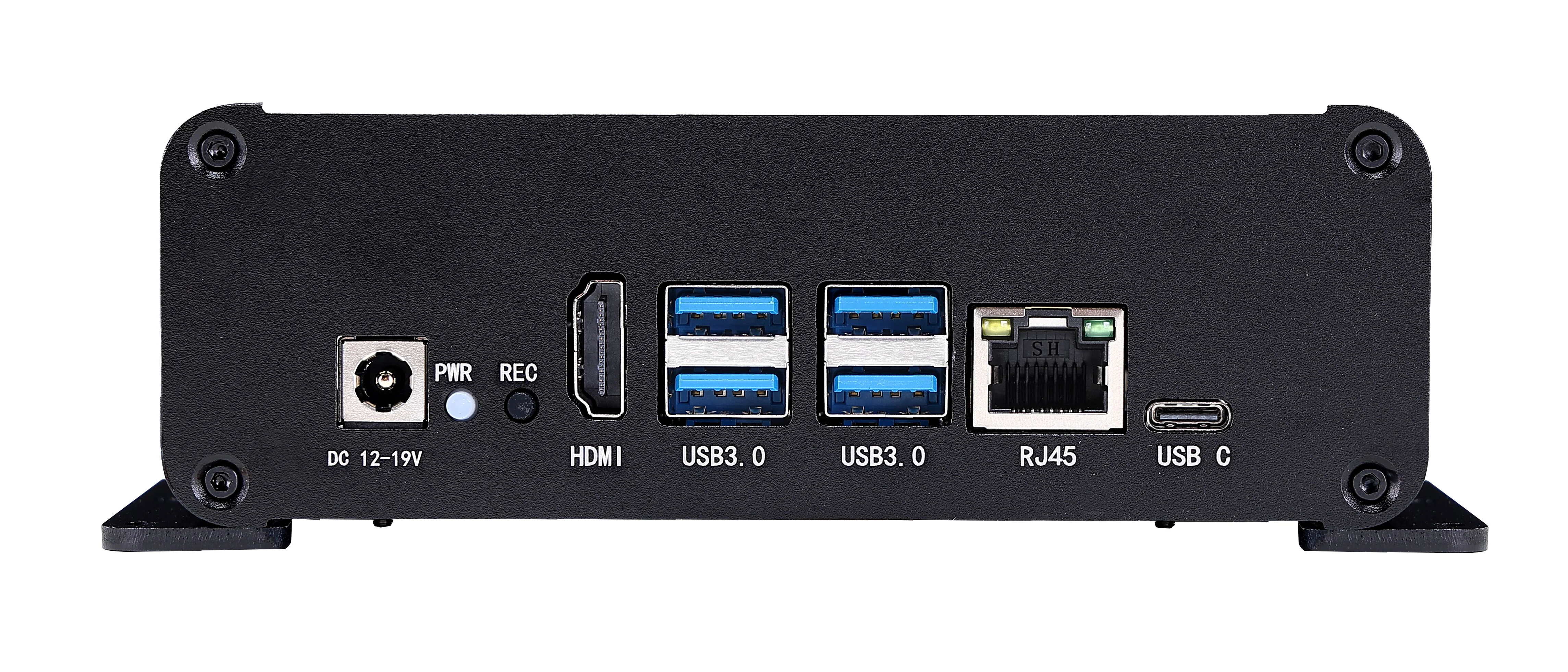
Figure 15. C1903 kit front view
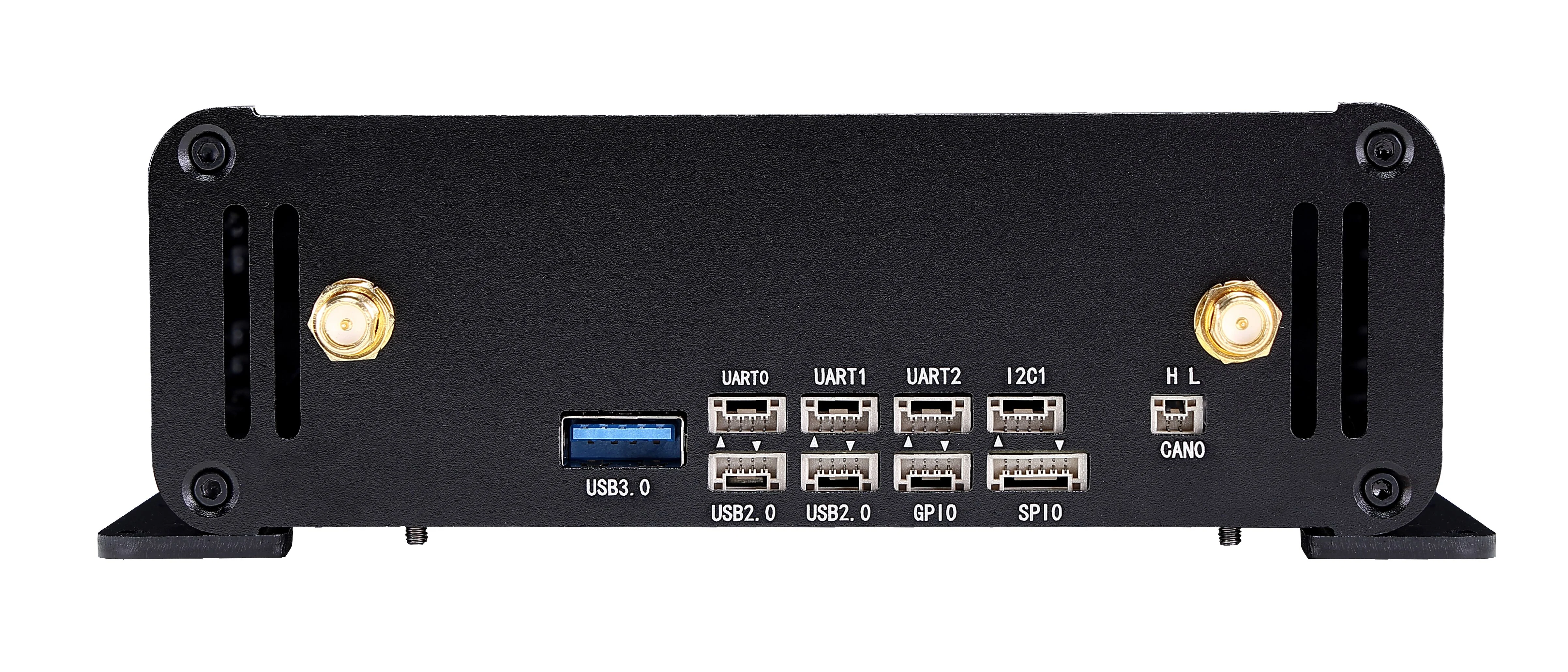
Figure 16. C1903 kit rear view
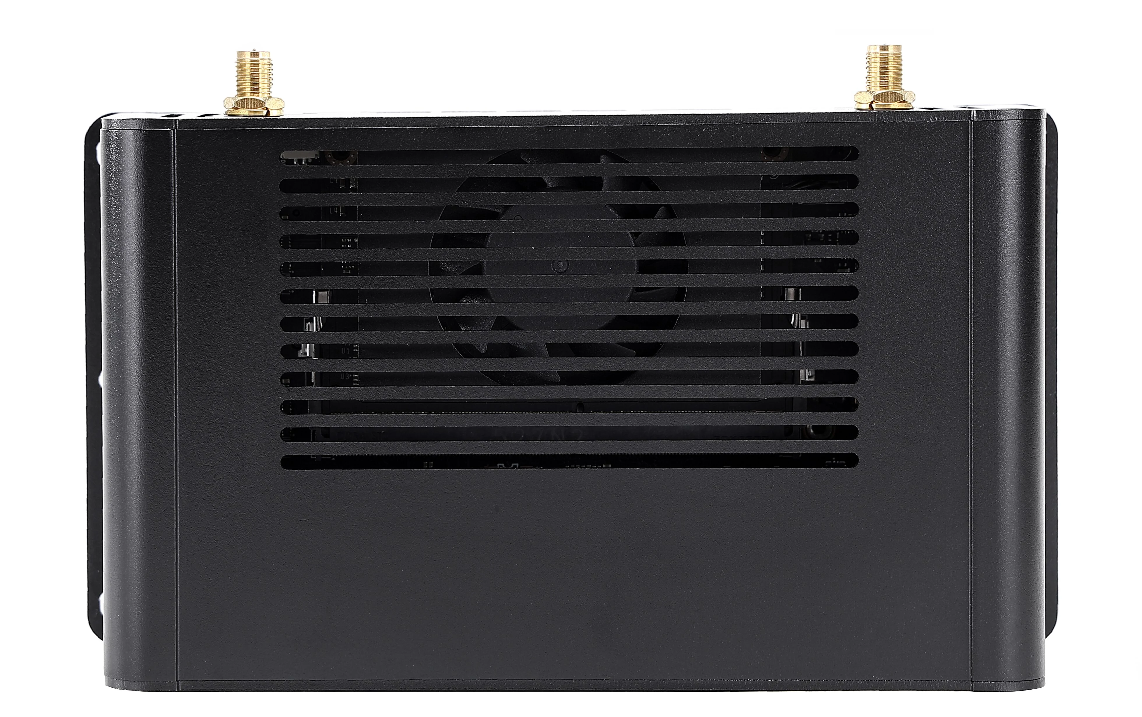
Figure 17. C1903 kit top view
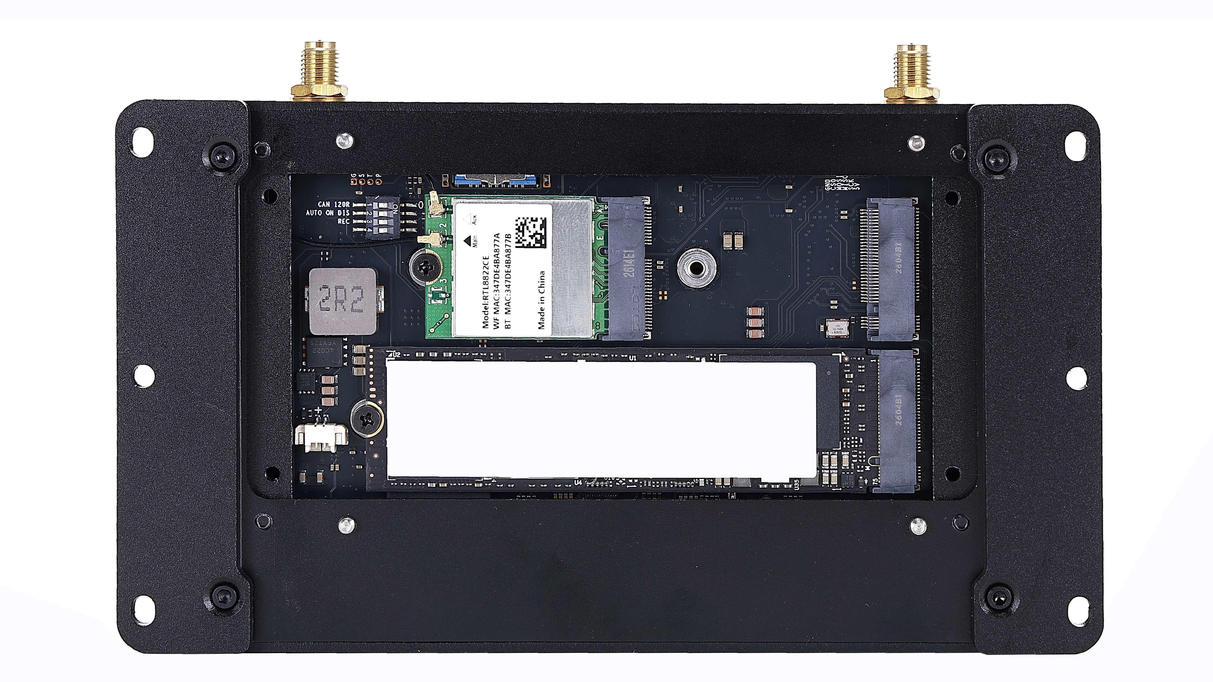
Figure 18. C1903 kit bottom, cover removed
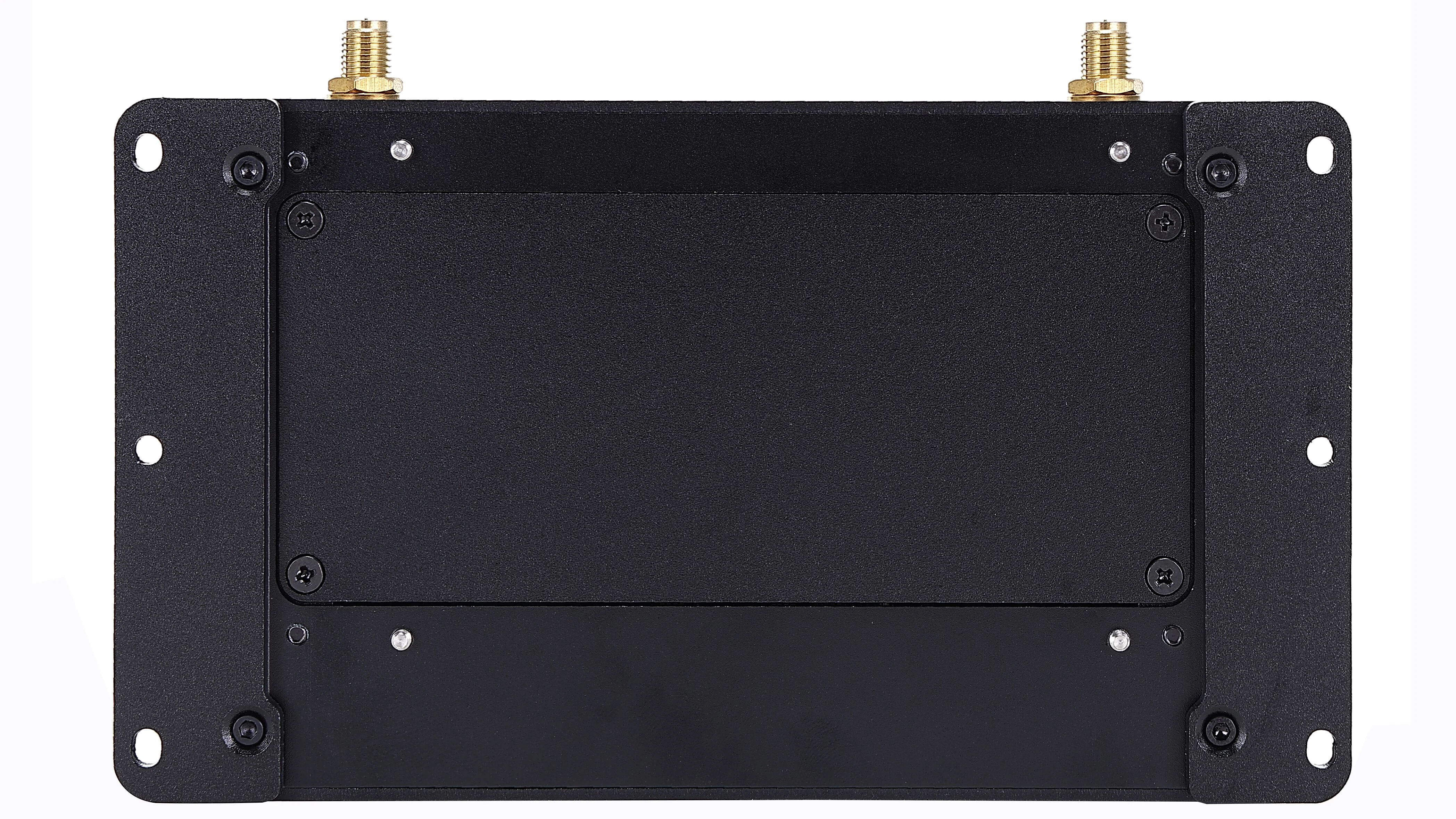
Figure 19. C1903 kit bottom with cover installed